
Plastic upscreening
Reliability testing for plastic encapsulated microcircuits
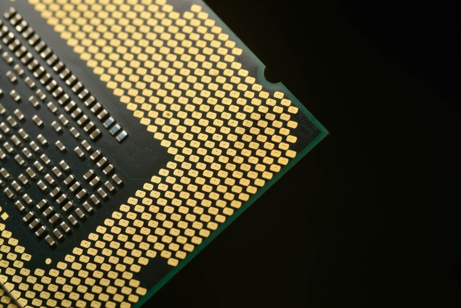
As ceramic and hermetic semiconductor packages become harder to procure, plastic packaged devices may be the most practical available route for maintaining long-life systems. However, a plastic encapsulated microcircuit (PEM) shouldn’t be treated as a like-for-like replacement for a hermetic or military-grade device. Package construction, moisture sensitivity, temperature performance and application requirements all need to be understood before a plastic device can be considered for use in a higher-reliability environment.
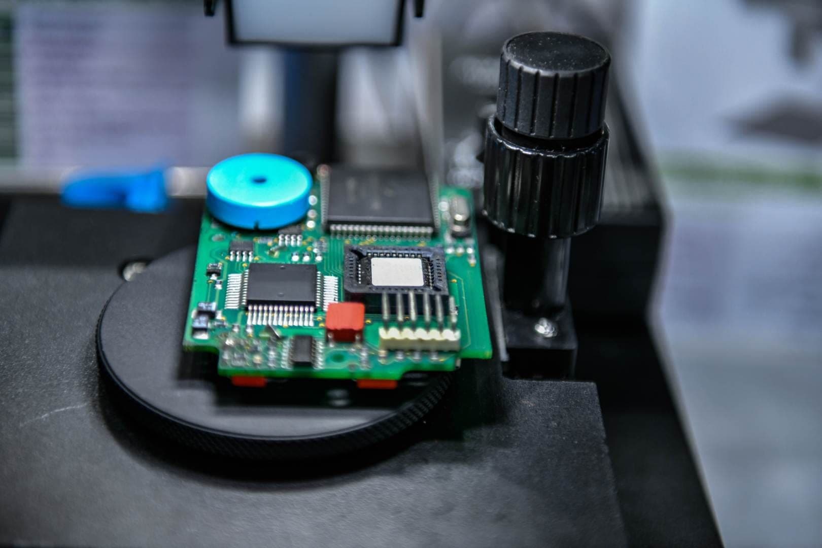
Force Technologies can help create a custom screening plan that exercises the device in question to ensure it is fit for use in your specific application. Alternatively, devices can be put through a MIL-PRF-38535 qualification which contains specific PEM screening flows depending on application criticality. Whether you just require temperature-based electrical screening, early life fail screening, full life testing or environmental testing, Force Technologies can provide the information to allow you to make evidence-led decisions.
Explore whether a plastic device is suitable for your application
MIL-PRF-38535M screening procedure
| Screening test | Class Y (ceramic or organic) — level S | Class N (PEM) — level B | Class P (PEM) — level S |
|---|---|---|---|
| Wafer lot acceptance test | QM plan (see H.3.2.1.4) 1/ or TM 5007 of MIL-STD-883 (all lots) | QM plan (see H.3.2.1.4) 1/ | QM plan (see H.3.2.1.4) 1/ or TM 5007 of MIL-STD-883 (all lots) |
| Nondestructive bond pull (NDBP) test 2/ | TM 2023 | — | — |
| Internal visual inspection 3/ | TM 2010, condition A | TM 2010, condition B | TM 2010, condition A |
| Temperature cycling 4/ | TM 1010, condition C, 10 cycles minimum or condition B, 15 cycles minimum | TM 1010, condition B, −55 to 125 °C, 15 cycles minimum | TM 1010, condition B, −55 to 125 °C, 15 cycles minimum |
| Constant acceleration 5/ | TM 2001, condition E (minimum), Y1 orientation only | — | — |
| Visual inspection 6/ | 100% | 100% | 100% |
| Particle Impact Noise Detection (PIND) test 7/ 8/ | TM 2020, test condition A on each device | — | — |
| Serialization 9/ | In accordance with device specification (100%) | In accordance with device specification (100%) | In accordance with device specification (100%) |
| Pre burn-in (interim) electrical parameters test 10/ | In accordance with device specification 12/ 25/ | In accordance with device specification 11/ | In accordance with device specification 12/ 25/ |
| Burn-in test 10/ 13/ 14/ | TM 1015, 240 hours at 125 °C, condition D 15/ | TM 1015, 160 hours at 125 °C | TM 1015, 240 hours at 125 °C, condition D 15/ |
| Post burn-in (interim) electrical parameters test 10/ | In accordance with device specification 12/ 25/ | — | In accordance with device specification 12/ 25/ |
| Reverse bias burn-in test (static burn-in) 13/ 14/ 16/ | TM 1015, condition A or C; 144 hours at +125 °C or 72 hours at +150 °C minimum | — | TM 1015, condition A or C; 144 hours at +125 °C or 72 hours at +150 °C minimum |
| Post burn-in (interim-reverse bias) electrical parameters test 10/ | In accordance with device specification 12/ 25/ | — | In accordance with device specification 12/ 25/ |
| Percent defective allowable (PDA) calculation 17/ | 5 percent PDA, 3 percent PDA for functional parameters at 25 °C (all lots) | 5 percent PDA (all lots) | 5 percent PDA, 3 percent PDA for functional parameters at 25 °C (all lots) |
| Final electrical tests 18/ — static, dynamic/functional 19/ and switching tests at 25 °C and maximum/minimum operating temperature | In accordance with applicable device specification (see group A test) 25/ 26/ | In accordance with applicable device specification (see group A test) | In accordance with applicable device specification (see group A test) 25/ 26/ |
| Seal test 20/ (a. fine leak, b. gross leak) | Not applicable | — | — |
| Radiographic (X-ray) and/or acoustic microscopy test 21/ | X-ray: TM 2012, two views; acoustic microscopy: TM 2030 | — | X-ray: TM 2012 |
| External visual inspection 22/ 23/ | TM 2009 | TM 2009 | TM 2009 |
| Qualification or quality conformance inspection / TCI test sample selection | 24/ | 24/ | 24/ |
Screening procedure for non-hermetic classes N, P and Y microcircuits. Test methods (TM) refer to MIL-STD-883; numbered references (e.g. 1/) refer to the notes in MIL-PRF-38535.
Frequently asked questions
Is plastic upscreening the same as standard upscreening?
Plastic upscreening is a more specific form of upscreening focused on plastic packaged devices. Standard upscreening may assess whether an available component can meet a higher grade or application requirement. Plastic upscreening also needs to account for package-specific factors such as moisture sensitivity, temperature performance and the suitability of the test flow for a non-hermetic device.
What does PEM mean?
PEM stands for plastic encapsulated microcircuit. It refers to a semiconductor device packaged in plastic rather than a traditional hermetic ceramic or metal package. PEMs are widely used and readily available in commercial and industrial applications.
What do ceramic, hermetic and plastic packages mean?
In semiconductor packaging, ceramic describes the package material, while hermetic describes the seal. Many high-reliability devices have traditionally used hermetic ceramic packages, which are designed to protect the die and internal connections from moisture and contamination. Plastic encapsulated microcircuits, or PEMs, use plastic packaging and are generally non-hermetic, so they behave differently under moisture, temperature and environmental stress. This is why plastic device upscreening needs an appropriate test flow rather than treating a plastic package as a direct equivalent to a hermetic ceramic device.
Considering a plastic part for a critical application?
Talk to our team about the right screening flow to assess a plastic encapsulated device for your programme.